Device illustration
Do more with fewer optical components
Meta-optics enabling non-Littrow gratings and monolithic devices for advanced beam shaping & dispersion control
Tech background SEM image solutions

System performance starts at the nanoscale

Beam shaping and high dispersion combined: Our non-Littrow gratings simultaneously deliver high angular dispersion and engineered beam profiles, achieving 2–5× higher wavelength resolution than conventional Littrow designs.
n-in-1 component integration: Starting with 3-in-1 integration, our meta-optics can scale to combine multiple beam-shaping and dispersive functions on a single monolithic optic, eliminating mounts and vibration-sensitive alignments.
Metasurface design: Patent-pending metasurface designs enable 90–100% efficiency across arbitrary incidence–deflection angles, with precise control over polarization sensitivity or insensitivity.
All-dielectric materials: Nano-fabricated optical devices are built without metals, polymers, epoxies, or gelatin, ensuring robustness under high optical power and temperature variation.
Foundry-ready process flow: Fabrication uses semiconductor foundry equipment and clean-room processes to enable high yield and eliminate lot-to-lot variation.
Tech background image wafer-scale technology

Meta-optics for nanoscale control of light

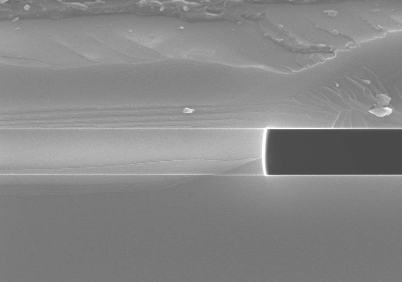
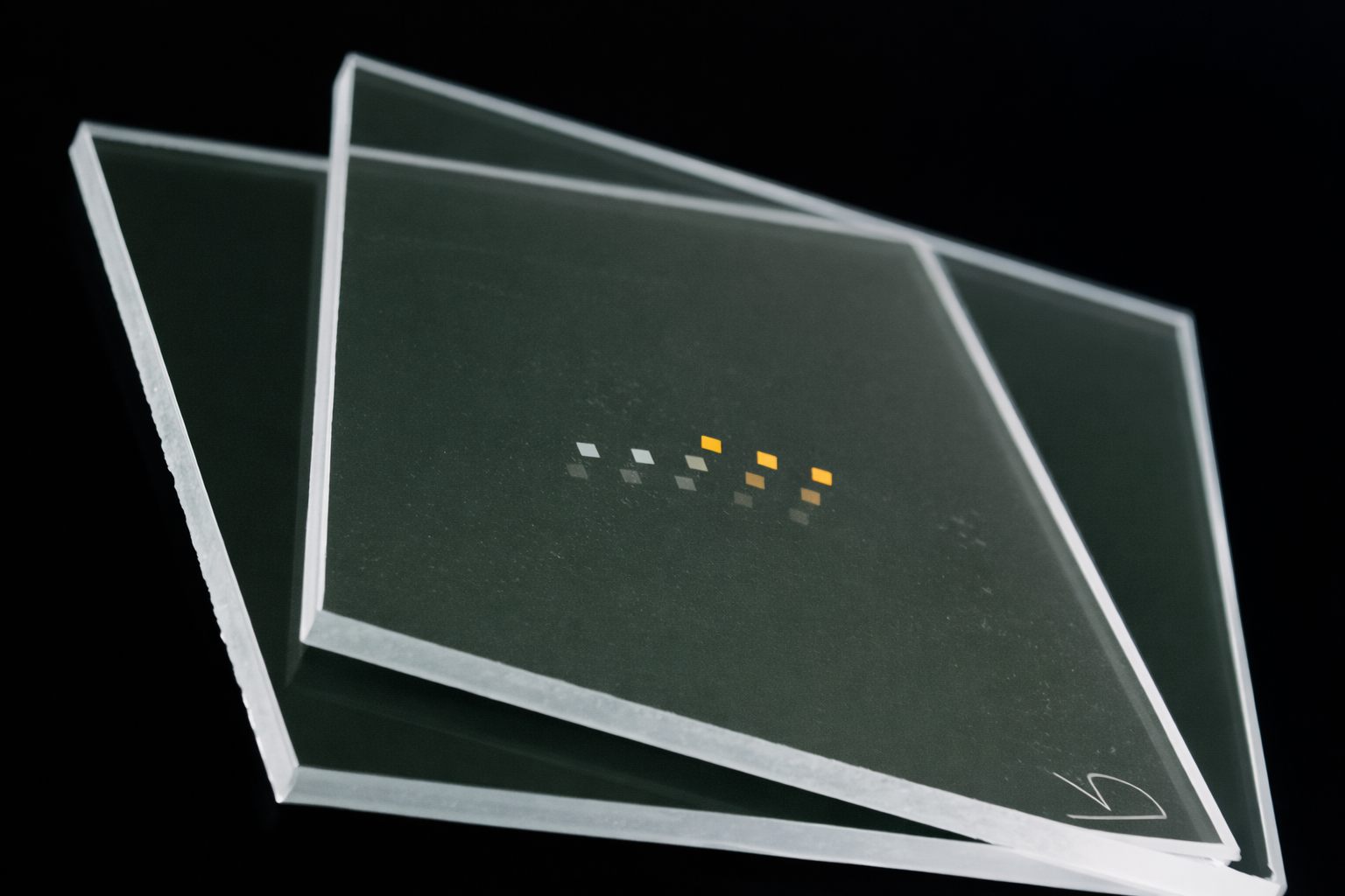
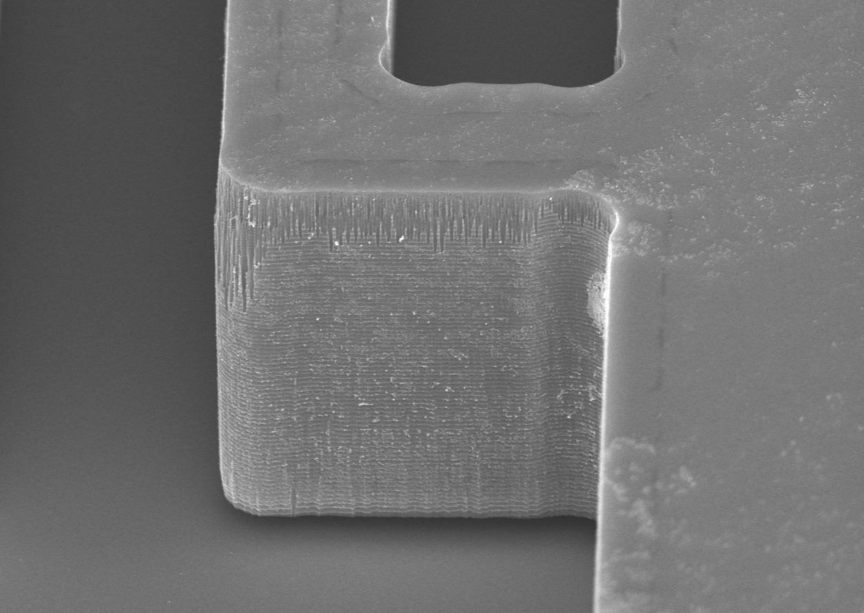
Metasurface optics, or simply meta‑optics, uses periodic arrays of nanostructures to create optical functions beyond what conventional optics can achieve. Our specialty lies in designing and fabricating nanoscale elements that function as unidirectional optical antennas—an optical analogue of the Yagi antenna. When illuminated, these antennas capture light within volumes far smaller than the wavelength of light. By precisely controlling how each antenna re‑emits light, the metasurface redirects the beam with a tailored wavefront. Our approach engineers strong light‑matter interactions at the nanoscale, delivering advanced beam shaping and dispersion control unattainable with conventional optics, as well as with phase‑gradient metasurfaces that rely primarily on wavefront shaping through surface‑relief modulation.

Tech background SEM image about

Delivering nanoscale control to macroscopic optical systems

We are a Canadian company based in Montréal, developing meta‑optics for OBMs and OEMs that require high‑performance beam shaping and dispersion control to overcome efficiency losses and footprint constraints. Our work follows a structured three‑stage process: design, prototype evaluation, and wafer‑scale production. We partner with established nanofabrication facilities worldwide to meet production needs while optimizing performance, timelines, and cost from early design through production.

Our team brings decades of experience in meta‑optics and light‑matter interaction, including contributors who have been active since the field’s early development. Our technology originated from research at Polytechnique Montréal and Concordia University and is supported by Québec’s optics and nanofabrication infrastructure.

Want to learn more about our technology or explore a collaboration? Contact our CEO, Ashutosh Patri (PhD, Polytechnique Montréal), our Business Development Advisor, Seth Coe-Sullivan (PhD, MIT), reach out via our LinkedIn page or email us at contact@epsilonphoton.com.